- 您现在的位置:买卖IC网 > Sheet目录472 > MAX2160EVKIT (Maxim Integrated)EVAL KIT MAX2160
�� �
�
�ISDB-T� Single-Segment� Low-IF� Tuners�
�ABSOLUTE� MAXIMUM� RATINGS�
�All� VCC_� Pins� to� GND............................................-0.3V� to� +3.6V�
�All� Other� Pins� to� GND.................................-0.3V� to� (V� CC� +� 0.3V)�
�RFIN,� Maximum� RF� Input� Power� ....................................+10dBm�
�ESD� Rating...........................................................................±1kV�
�Short-Circuit� Duration�
�IOUT,� QOUT,� CPOUT,� XTALOUT,� PWRDET,� SDA,�
�TEST,� LTC,� VCOBYP� ...........................................................10s�
�Continuous� Power� Dissipation� (T� A� =� +70°C)�
�40-Pin� Thin� QFN� (derate� 35.7mW/°C� above� +70°C)....2857mW�
�WLP� (derate� 10.8mW/°C� above� +70°C).........................704mW�
�Operating� Temperature� Range� ...........................-40°C� to� +85°C�
�Junction� Temperature� ......................................................+150°C�
�Storage� Temperature� Range� .............................-65°C� to� +150°C�
�Lead� Temperature� (soldering,� 10s)� .................................+300°C�
�CAUTION!� ESD� SENSITIVE� DEVICE�
�Stresses� beyond� those� listed� under� “Absolute� Maximum� Ratings”� may� cause� permanent� damage� to� the� device.� These� are� stress� ratings� only,� and� functional�
�operation� of� the� device� at� these� or� any� other� conditions� beyond� those� indicated� in� the� operational� sections� of� the� specifications� is� not� implied.� Exposure� to�
�absolute� maximum� rating� conditions� for� extended� periods� may� affect� device� reliability.�
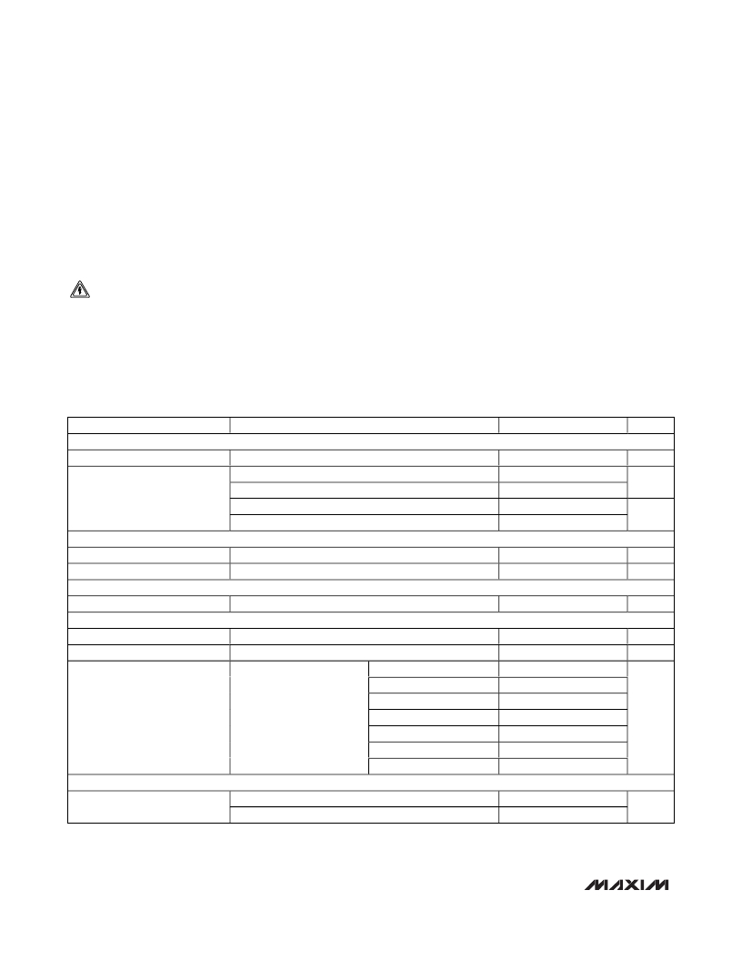
�DC� ELECTRICAL� CHARACTERISTICS�
�(MAX2160� EV� kit,� V� CC� =� +2.7V� to� +3.3V,� V� GC1� =� V� GC2� =� 0.3V� (maximum� gain),� no� RF� input� signals� at� RFIN,� baseband� I/Os� are� open�
�circuited� and� VCO� is� active� with� f� LO� =� 767.714MHz,� registers� set� according� to� the� recommended� default� register� conditions� of�
�Tables� 2–11,� T� A� =� -40°C� to� +85°C,� unless� otherwise� noted.� Typical� values� are� at� V� CC� =� +2.85V,� T� A� =� +25°C,� unless� otherwise�
�noted.)� (Note� 1)�
�PARAMETER�
�CONDITIONS�
�MIN�
�TYP�
�MAX�
�UNITS�
�SUPPLY�
�Supply� Voltage�
�Supply� Current� (See� Tables� 15�
�and� 16)�
�Receive� mode,� SHDN� =� V� CC� ,� BBL[1:0]� =� 00�
�Standby� mode,� bit� STBY� =� 1�
�Power-down� mode,� bit� PWDN� =� 1,� EPD� =� 0�
�Shutdown� mode,� SHDN� =� GND�
�2.7�
�2.85�
�44�
�2�
�5�
�0�
�3.3�
�53.5�
�4�
�40�
�10�
�V�
�mA�
�μA�
�ANALOG� GAIN-CONTROL� INPUTS� (GC1,� GC2)�
�Input� Voltage� Range�
�Input� Bias� Current�
�Maximum� gain� =� 0.3V�
�0.3�
�-15�
�2.7�
�+15�
�V�
�μA�
�VCO� TUNING� VOLTAGE� INPUT� (VTUNE)�
�Input� Voltage� Range�
�0.4�
�2.3�
�V�
�VTUNE� ADC�
�Resolution�
�3�
�bits�
�Input� Voltage� Range�
�110� to� 111�
�101� to� 110�
�100� to� 101�
�0.3�
�V� CC� -� 0.4�
�1.9�
�1.7�
�2.4�
�V�
�Reference� Ladder� Trip� Point�
�ADC� read� bits�
�011� to� 100�
�1.3�
�V�
�LOCK TIME CONSTANT OUTPUT� (LTC)�
�010� to� 011�
�001� to� 010�
�000� to� 001�
�0.9�
�0.6�
�0.4�
�Source� Current�
�Bit� LTC� =� 0�
�Bit� LTC� =� 1�
�1�
�2�
�μA�
�2�
�_______________________________________________________________________________________�
�发布紧急采购,3分钟左右您将得到回复。
相关PDF资料
MAX2163ETI/V+
IC TUNER ISDB-T LOW IF 28TQFN
MAX2165EVKIT+
KIT EVAL FOR MAX2165
MAX2170EVKIT+
KIT EVAL FOR MAX2170
MAX2202EWT+T
IC POWER DETECTOR RMS 6-WLP
MAX2203EWT+T
IC RMS PWR DETECTOR 6WLP
MAX2204EVKIT+
KIT EVAL FOR MAX2204
MAX2205EVKIT+
KIT EVAL FOR MAX2205
MAX2209AEBS+T
IC RF PWR DETECTOR 4UCSP
相关代理商/技术参数
MAX2161E/W-B3N
功能描述:调谐器 RoHS:否 制造商:NXP Semiconductors 功能: 噪声系数: 工作电源电压: 最小工作温度: 最大工作温度:
MAX2161ETL+
功能描述:调谐器 ISDB-T 1&3-Seg Low-IF Tuner RoHS:否 制造商:NXP Semiconductors 功能: 噪声系数: 工作电源电压: 最小工作温度: 最大工作温度:
MAX2161ETL+T
功能描述:IC TUNER ISDB-T LOW IF 40TQFN RoHS:是 类别:RF/IF 和 RFID >> RF 其它 IC 和模块 系列:* 标准包装:100 系列:*
MAX2161EVKIT+
功能描述:射频开发工具 MAX2161/62 Eval Kit RoHS:否 制造商:Taiyo Yuden 产品:Wireless Modules 类型:Wireless Audio 工具用于评估:WYSAAVDX7 频率: 工作电源电压:3.4 V to 5.5 V
MAX2161SEVKIT
功能描述:射频开发工具 MAX2161S Eval Kit RoHS:否 制造商:Taiyo Yuden 产品:Wireless Modules 类型:Wireless Audio 工具用于评估:WYSAAVDX7 频率: 工作电源电压:3.4 V to 5.5 V
MAX2161SEWA+T
功能描述:调谐器 ISDB-T 1&3-Seg Low-IF Tuner RoHS:否 制造商:NXP Semiconductors 功能: 噪声系数: 工作电源电压: 最小工作温度: 最大工作温度:
MAX2162ETL+
制造商:Rochester Electronics LLC 功能描述: 制造商:Maxim Integrated Products 功能描述:
MAX2162SEVKIT+
制造商:Maxim Integrated Products 功能描述:ISDB-T1-AND 3-SEGMENT LOW - IF TUNERS - Rail/Tube